
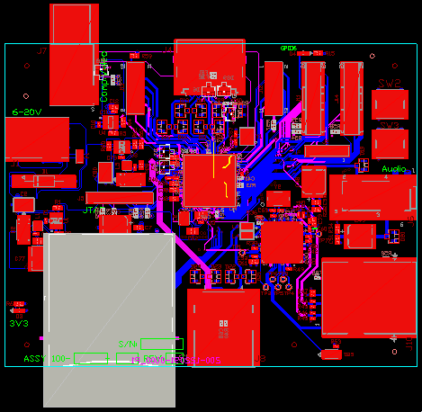
The Raspberry Π computer is an example of what I discussed before about the ability to go from CAD to functionality so easily. It goes from concept to device and I understand it is ARM with Linux and that is something I just recently came up to speed on as well as the interface specs for various connection protocols. The next step is to integrate electronic substrate manufacture which would allow a completely fabless implementation that would be less than the price of a candy bar.
Considering that this is a fully functioning device which would have been the size of an office building in the 60's it gives some sense of what is possible in the future. Fifty years of miniaturization has the scale of fab at 9 nanometers possible though 45 nanometers is the current deliverable AFAIK. Even a 5x scaling like this leads to a 125x change in the 3D bonded out unit. This can mean that it can be the size of a pea and the power of an old super computer. Nanosphere lithography, which may be the future is similar to some techniques I have investigated.
It does seem that it may come delivered with its own CAD, which can create its own circuits and that would be a boundary condition. If it can expand on its own with the addition of material, it could easily be the end of the mechanical aspect of the industry.
It seems that Raspberry went from idea to physicality in less than a month. That is definitely a "singularity" like effect as many designs that I was involved in as late as 1987 required massive capital, many engineers and years of planning. It is not just the size of the devices that influences utility, but the design cycle, cost, and transitional cost. So, a design that is 125x actually is closer to 10,000 times more effective.
It is not unreasonable to consider a 3D bond-out method that uses the same techniques as chip only technology. Given an FPGA framework and the appropriate CAD methods it could produce a continuously variable and reconfigurable matrix that could be constructed on the fly as well as decomposed and reconfigured.
There is no reason not to deliver the silicon with its own CAD/CAM in the same way that flash cpus have their own built-in monitor program to accept serial programming.
The effective use of this type of technology comes in its ability to be applied in a ballistic and parallel manner. It is similar to wiring a biological brain. If you have a circuit assembly with the ability to perform 3D connection and reconnection then it can become a real time problem solver. It is obvious we are proceeding toward the reality of replicators, but is not the same as the science fiction hype. I have yet to see any 20 foot ants that have evolved from atomic bomb testing and I actually don't expect that we ever will. The design cycle is very short and I can see that if I applied myself to this, I could generate a usable analogy to a biological brain with a 18x18 mouse image chip and some FPGAs. It probably could be done in a week to a functioning prototype.
The possible futures are far more than have been presently considered and certainly not planned against. It might be interesting to use an MRI and a direct 3D transfer of circuit from something as simple as an immortal worm and as an added bonus do the ballistic Markov chains that bind the DNA to be operated at light speeds. Hmmmm... that is an interesting sub idea, maybe next week.

0 comments:
Post a Comment